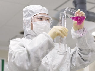
Research & Development
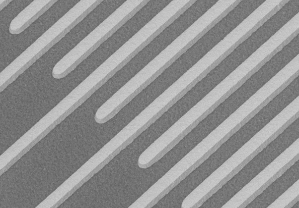
Laser direct imaging system
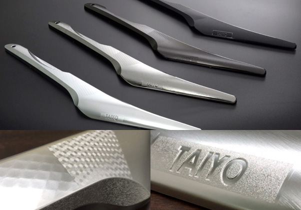
Production of Plastic molding
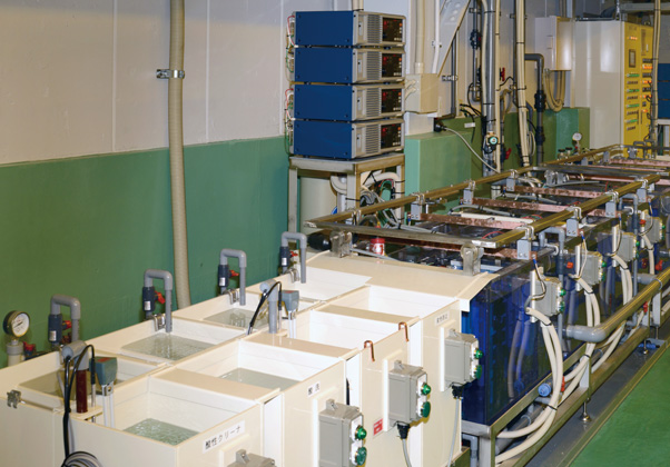
Plastic Plating
Painting, laser Etching and assembly
Complete Chrome-Ⅵ free
Silica-based Coating
Electroless Ni-Au plating, terminal plating and bond Au plating
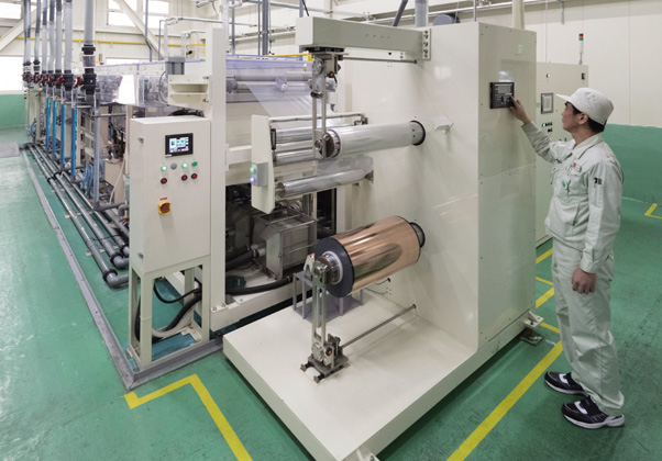
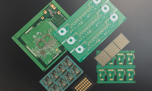
Flexible board: drilling, through-hole copper plating, gold plating
Electronic Circuit Board: through-hole copper plating
Bump plating
Ceramic board plating
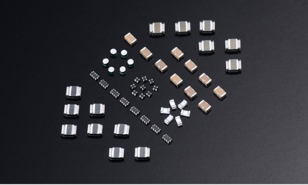
Plating for SMD terminals
Ni-hoop plating (secondary battery Electrode)
Zinc and zinc-nickel plating
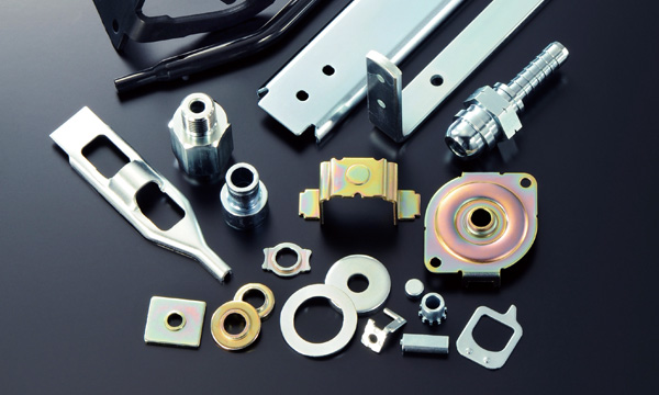
Nickel and tin plating
Alumite and alodine
Gold and silver plating
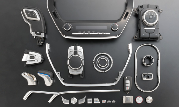
You can find Taiyo products everywhere
 In Cars
 smart phones
 houses
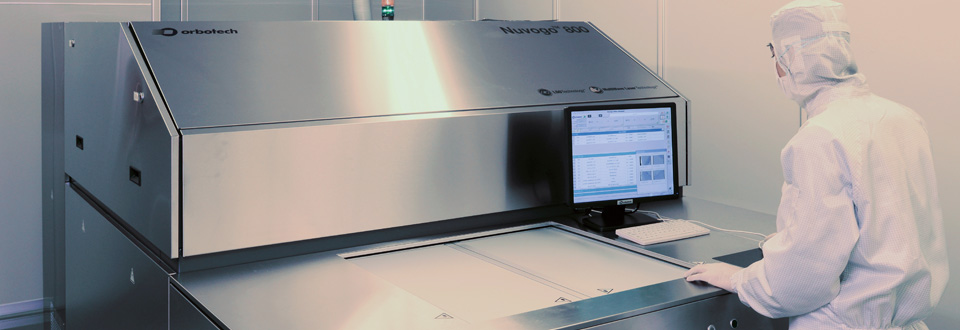
Laser direct imaging system

Taiyo has devoted to the technological development of the high precision plating, which is indispensable for mounting of semiconductor devices and other electric components.As a pioneer in the field, we succeeded in the processing of the solder bump plating on the silicon wafers.In the bump process of TAIYO, with our original plating devices, various metals such as gold, solder, and Pb free solder can be formed not only on the wafer but also on a printed circuit board and a ceramic base. Moreover, some former processes such as the UBM process and the Photo Lithography process are available at TAIYO.The precise function plating of Taiyo keep supporting the mounting technologies of the semiconductor parts in this rapid changing field.